Lab 2: Multiplexed 7-Segment Display
Introduction
The goal of this design is to practice multiplexing by designing a FPGA that can take two 4-bit inputs and 1) show their hexadecimal values with a dual 7-segment display and 2) show their sum in binary with 5 LEDs. The constraint is that only one 7-segment decoder module can be used for both digits on the display, resulting in the need of time-multiplexing.
Design
The top level design, lab2_gt, included three modules: the on-board high-speed oscillator (HSOSC) from the iCE40 UltraPlus primitive library, a clock divider to toggle or select between the digits shown on the display, and a 7-segment display decoder. The general idea of the design can be visualized with the block diagram below:
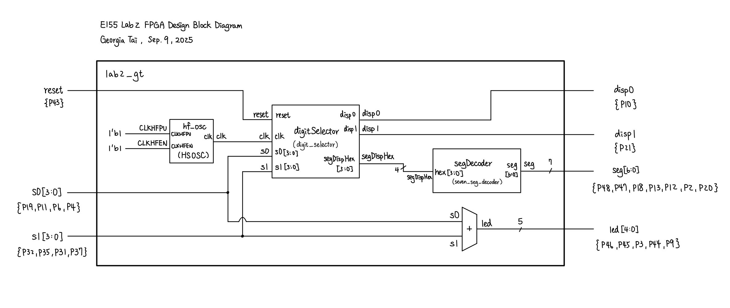
The clock divider, digitSelector, selects the digit which will be displayed on the dual 7-segment display with 60 Hz. The frequency was chosen such that the human eyes can not catch that the two digits are turning on and off, creating the illusion that both digits are always on at the same time. The module achieves such frequency by taking in a 48 MHz clock input clk given by the high-speed oscillator and using a counter incremented at each clock cycle to toggle the enabling signal for each digit at 60 Hz. It then outputs both enabling signals and the 4-bit binary of the digit with the enabled signal.
The 7-segment display decoder contains a set of combinational logic to translate a 4-bit binary signal into a single hexadecimal value. Each segment of the display is a LED controlled by an I/O pin from the UPduino board, and the shape of each hexadecimal value is unique. As per the constraint of this lab, this module is only used once and takes the 4-bit binary input of the selected digit given by digitSelector.
In terms of the circuitry design, the dual 7-segment display was externally accessed on a breadboard, with each of its two common anode connected to a 2N3906 PNP transistor to provide enough current. Other than the switch located on the PCB provided by the course, SW6, an external 4-input switch was also wired ono the breadboard. The switch on the PCB controls the left digit, whereas the one on the breadboard controls the right digit. The 5 LEDs for showing the sum are also connected on the breadboard. The schematics for the physical circuit design is shown in the following graph:
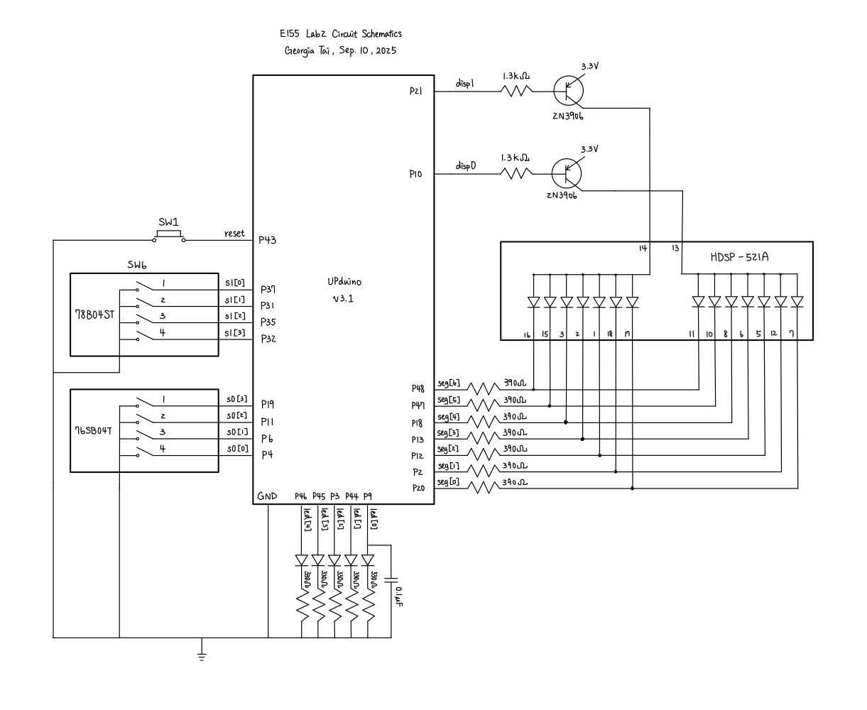
For the LEDs display is the sum, I chose to use red LEDs, whose forward voltage is normally around 1.6 V. Aiming for around 5 mA of current, which should provide enough brightness and is well below the maximum current of both the I/O pin of the UPduino (8 mA, found in section 4.17 of the datasheet) and the LED (20 mA conventionally), the resistor values for each LED can be calculated with:
\[ R_{LED} = \frac{3.3V - 1.6V}{0.005A} = 340 \Omega \]
The closest resistor I found was \(330 \Omega\), which should not affect the current much.
The datasheet of the 2N3906 transistor shows that it has a base-emitter saturation voltage of 0.65 to 0.85 V when the current through the base is 1 mA. Aiming for a current slightly smaller than that to ensure safety, say 0.8 mA, the resistor value is:
\[ R_{transistor} = \frac{V_{PIN} - V_{BE,SAT}}{I_{transistor}} = \frac{3.3V - 0.65V}{0.007A} \approx 380 \Omega \]
The closest resistor I found was \(390 \Omega\), which should not affect the current much.
A resistor value of \(220 \Omega\) are chosen considering the voltage and current across the LEDs. According to the dual 7-segment display datasheet, the voltage drop across the segments are about 1.8 V. The input voltage is the voltage given by the transistor, which is 2.6 V.Given that the collector-emitter saturation voltage was 0.4 V and aiming for approximately 5 mA across the LEDs of the segments, the resistor value is:
\[ R_{seg} = \frac{(V_{PIN} - V_{CE,SAT}) - V_{seg}}{I_{seg}} = \frac{(3.3V - 0.4V) - 1.8V}{0.005A} = 220 \Omega \]
Testing and Results
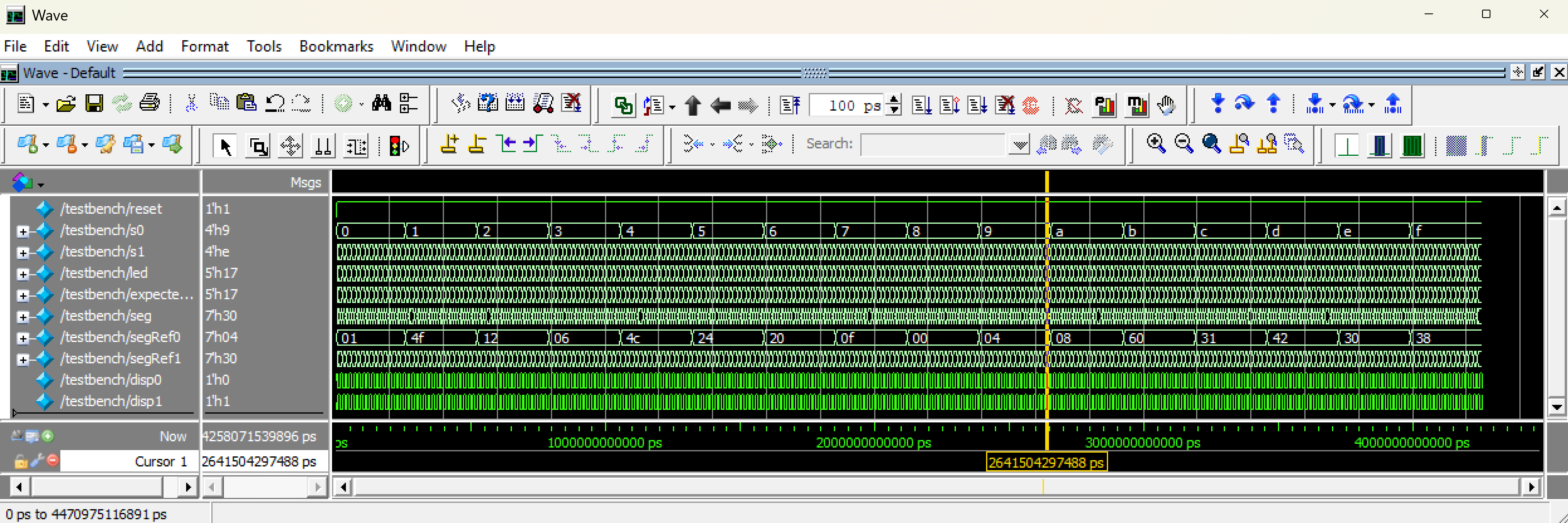
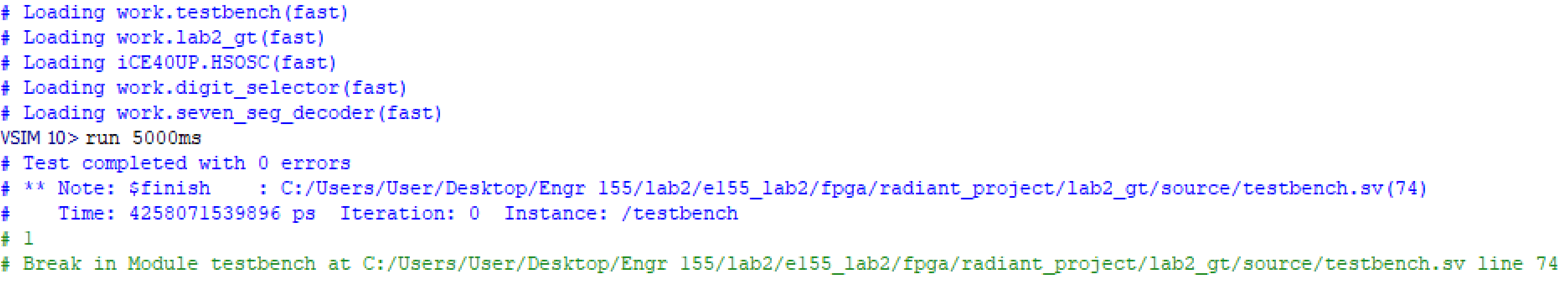
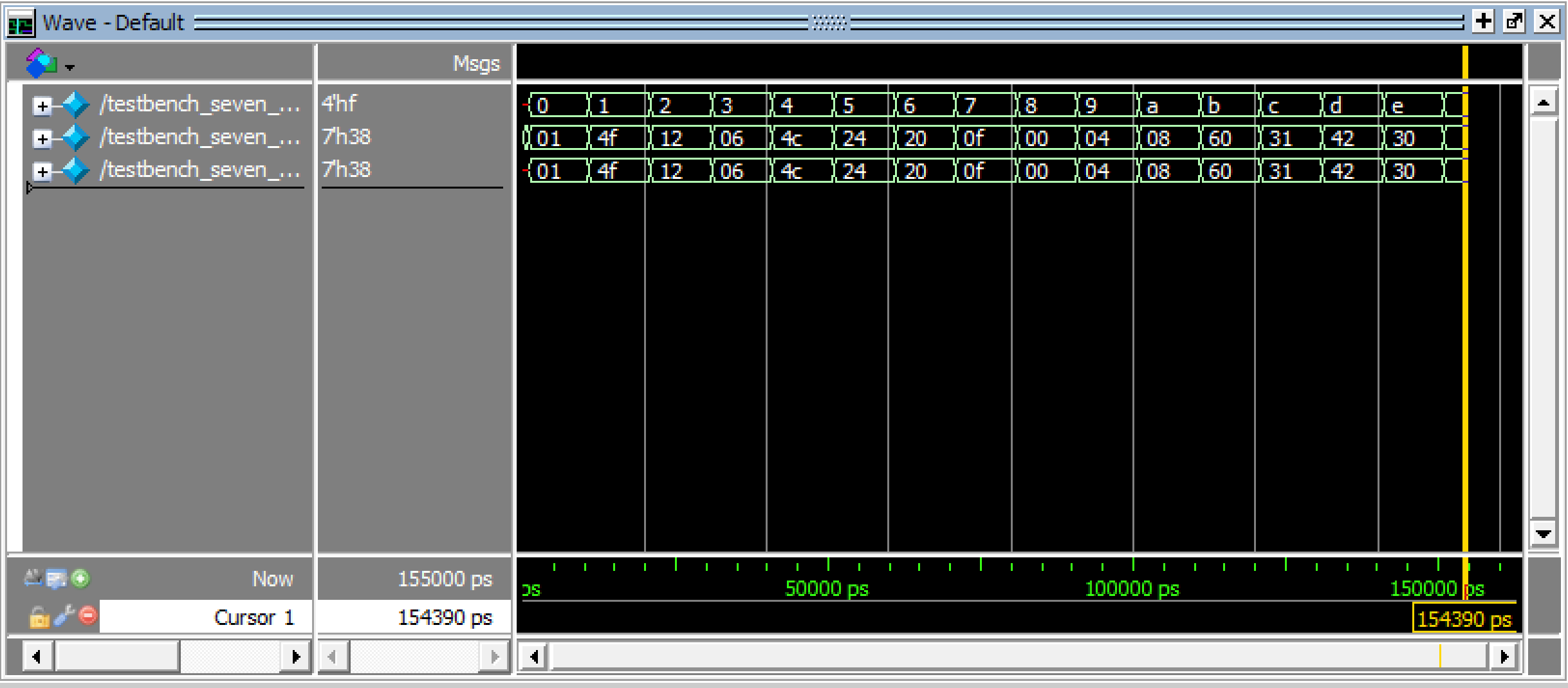
Each of the modules are testes with automated testbenches. The top level module was tested using a for-loop to stimulate all 256 (4-bit input s0 * 4-bit input s1), checking that the outputs for segments are correct when the enabling signal for each digit, disp0 and disp1, is on. The seven segment display decoder is identical to Lab 1, checking the combinational logic for all 16 possible inputs. The clock divider/digit selector checks that the enabling signals actually toggles and select the correct input for the 7-segment decoder after an expected amount of time.
Using Questa to simulate, the following figures show that All modules have successfully passed their testbench.
lab2_gt

seven_seg_decoder
After verifying the code with testbenches, the circuit which I built also has to be tested. There was no obvious blinking or toggling between the two digits, and output for both the display and the LEDs are correctly shown. Here is a picture of the complete device.

Conclusion
In this lab, I successfully designed and built an FPGA design that was able to correctly display hexadecimal values of two 4-bit binary input with only using one 7-segment decoder module. There was no observable blinking between the two digits. The binary sum of the two 4-bit inputs was also correctly shown with 5 LEDs. Therefore, I believe that my design for this lab meets all the requirements of this lab. This week, I spent 8 hours on the lab. Design did not take much time, but writing the testbenches and wiring up the circuits took a good amount of time. I hope to become more proficient in writing testbenches and be more aware of what should be tested in a design.
AI Prototype Summary
For this AI prototype, I used ChatGPT. When feeding it the first prompt, the resulted design was able to synthesize the first time, surprisingly. By looking at the code, this design seemed somewhat similar to what I did, and seemed like is functionable. However, this design did assume clk to be an external input, and kept the counter in the top level module instead of in an independent module. One thing that I like about its design was that it did include a parameter in the top level module, allowing easy changes to the frequency which the two digits toggle.
For the second prompt, since my counter module from Lab 1 was more than a clock divider and thus did not fit this purpose, I modified the prompt and asked it to:
Write SystemVerilog HDL to time multiplex a single seven segment decoder (that decodes from four bits to a common anode seven segment display) to decode two sets of input bits and drive two sets of seven output bits. Use the seven segment decoder provided in the attached files and the HSOSC from the iCE40UP library.
The thinking time of this prompt was around 30 seconds, which was two times longer than the thinking time of privious prompt. When synthesizing it, it got this error:
Error 35901282 Synthesis ERROR <35901282> - c:/users/user/desktop/engr 155/lab2/e155_lab2/fpga/radiant_project/ai_2/source/impl_1/top.sv(67): loop count limit exceeded forever never breaks. VERI-1282 [top.sv:67]
This error came from the ifdef-elsif-else statement which this design provide. ChatGPT said the purpose of it was to include common ways to instantiate an on-chip oscillator and allows the user to choose which one by using the `ifdef. However, it was pretty redundant and got stuck on its approach of instantiate the clock if there is no on-chip oscillator:
forever #10 clk_hf = ~clk_hf;
It also made the same mistake of using SB_HFOSC instead of HSOSC in Lab 1. After asking it to remove the ifdef-elsif-else statement and assuming that the osciallator will be instantiate with one method, the new design was able to synthesize, and seemed like would work fine when I read through it.