Project Proposal
Julia Gong and Georgia Tai
Project Description
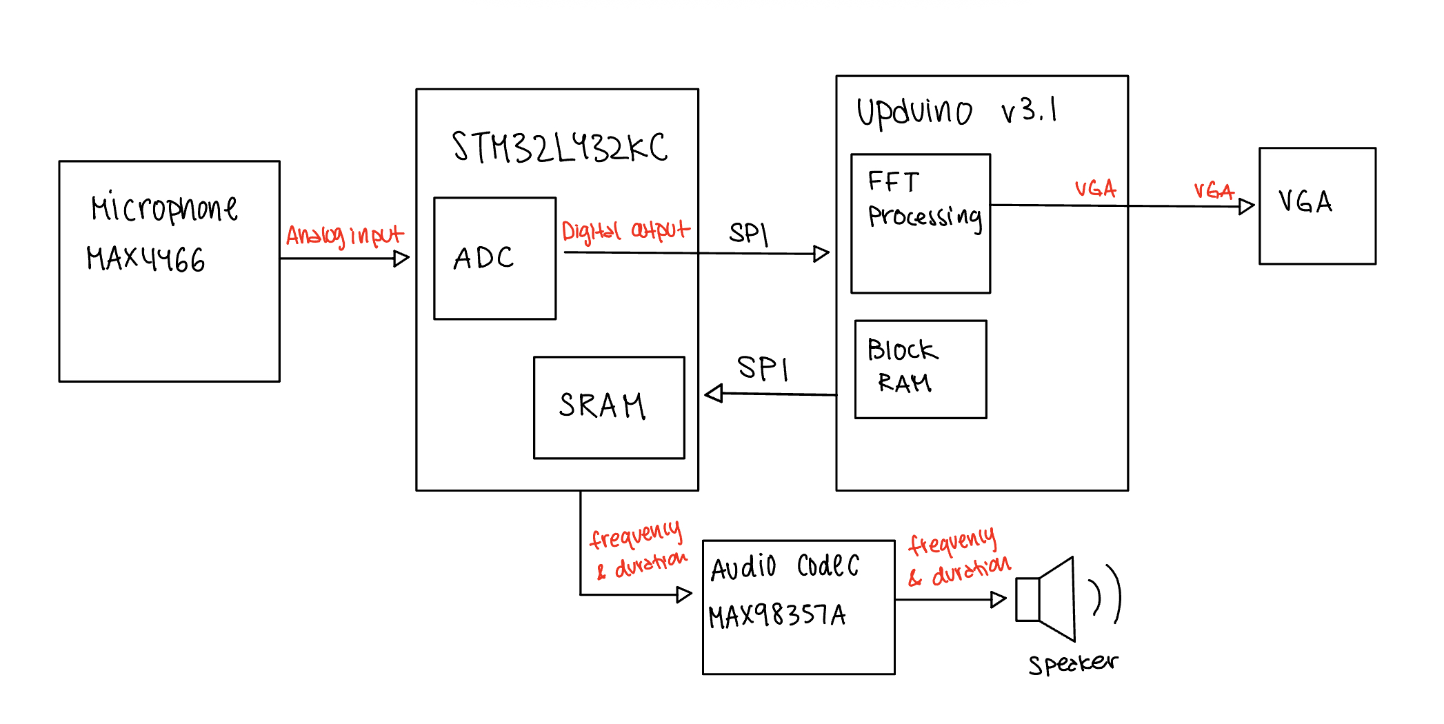
This project aims to take in sound inputs, whether using a keyboard, any instruments, or someone signing, transcribe the sound onto a score in real-time with a given bpm, and play back the input melody. An FPGA will be used as the main calculation and display engine, using Fast Fourier Transform (FFT) to handle frequency analysis and driving a VGA display. A MCU will be used for interfacing the audio inputs and outputs.
On the hardware level, an analog microphone will take in sounds, where the MCU will convert them into digital signals using ADC and send the converted signals to the FPGA. The MCU will then send the digital signals to the FPGA using SPI. Then, the FPGA will use FFT to extract the frequency and duration of the note inputted. The array of notes will then be used by the FPGA to calculate the pixels for displaying the score on a VGA display. This array of notes, after transcription ends, will be sent to the MCU through SPI to generate the playback audio. The user should be able to control the music transcription and play back audio with a hardware components such as a switch or a button, and control the volume with a potentiometer.
Project Specifications
Input: detection and analysis
- User can stop and start transcription using physical hardware (e.g. switch/button)
- System converts analog microphone signals into digital
- Uses FFT to extract clear signal from input
- System calculates input frequency and rounds to the nearest half note (e.g. A3#, C4)
- System able to detect duration accurate to 1/16 beat at the given BPM
Output: display and audio
- Display updates at > 24 Hz
- Note durations are displayed for 120 BPM
- Notes are displayed on VGA monitor ~75 ms after note is released
- Playback audio resembles the input
- Playback audio uses an audio codec so that output sound is not square wave
- User can control the volume of playback audio
- User can control when to playback the transcribed audio (e.g. switch/button), but can only play the audio when transcription is stopped
Design Overview
The input signals from the microphone remain the riskiest element of the system. To improve the microphone input detection, the Maxim MAX4466 was chosen since it has a built in amplifier with a maximum adjustable gain of x125.
FPGA: UPDuino v3.1 (iCE40UP5K)
- FFT & Pitch Detection - A 512-point FFT will be run by the FPGA to extract dominant frequencies from the digital audio samples sent from the MCU over SPI. The results will be stored in DPRAM.
- Duration Detection - The FPGA will count the FFT frames of a specific note and convert the count using the current BPM to infer duration of a note. The array of note events will also be stored in DPRAM.
- VGA Controller - VGA timing signals and framebuffer data extracted from DPRAM will be used to compose the score on a VGA screen in real time.
- SPI Peripheral - This provides the FPGA as an SPI interface which the MCU can read and write to, bridging the connection between the two.
MCU: STM32L432KC
- ADC - The microphone specifies to connect its output to the ADC pin. This will allow the MCU to buffer the samples and convert our desired input in to digital signals.
- I2S - This will allow the MCU to synthesize the audio for playback and send it to the audio codec, where the audio codec we chose to use expects I2S.
- Control - The MCU will handle user commands, reading buttons/switches for the start/end of transcription or playback and potentiometer for the volume of the playback audio.
- SPI Controller - The MCU will act as the SPI controller to send digital sound inputs to the FPGA and to receive the transcribed note array when transcription stops.
Calculations
Delay for Note Display
The shortest note that our system will recognize is a 16th note. Given 120 BPM, the length of a 16th note is 0.125 seconds. Therefore, the delay between the end of the note to when it is displayed on the VGA display must be less than 0.125 seconds so that a 16th note can be processed.
The total latency of our system can be estimated by: \[ T_{total} = T_{samplingWindow} + T_{spi} + T_{fft} + T_{postProcessing} + T_{display} \]
where the audio is sampled at 48 kHz such that \(T_{samplingWindow} = 512/48000 = 10.67 \text{ ms}\). SPI communication between the MCU and FPGA is set to sending 12 bit precision at 4 Mhz such that \(T_{spi} = 0.00025 \text{ ms} \times 12 \text{ bits} \times 512 \text{ samples} = 1.536 \text{ ms}\). The 512-point FFT requires 2304 butterfly operations, where 2 butterfly operations will be pipelined. There will be 1152 cycles. The FPGA will operate at 8MHz such that \(T_{fft} = 1152 \times 0.000125 \text{ ms} = 0.144 \text{ ms}\). Buffer time for post processing is estimated such that \(T_{display} = 2 \text{ ms}\). The VGA will be refreshing at a rate of 60 Hz, such that \(T_{display} = 16.7 \text{ ms}\).
Therefore, \[ T_{total} = 10.67 \text{ ms} + 1.536 \text{ ms} + 0.144 \text{ ms} + 2 \text{ ms} + 16.7 \text{ ms} = 31.05 \text{ ms} \]
To give flexibility with our note display, the estimated expected delay for each note should be 75 ms.
Fast Fourier Transform Calculations
The Fast Fourier Transform transforms a signal from the time to frequency domain by recursively dividing a discrete fourier transform (DFT) into its odd and even indexed elements. The odd and even DFTs are of size N/2, where N is the size of its non-spit DFT. Using the symmetry and periodicity properties of complex exponentials, the even part corresponds to a half sized DFT and odd part corresponds to a half sized DFT that is multiplied by the twiddle factor (which is complex exponential expressed by \(W_N\)).
These equations below show the DFT and how the DFT can be split into its even and odd components.
DFT equation: \[ X[k] = \sum_{n=0}^{N-1} x[n] W_N^{kn} \] DFT equation split into even and odd components: \[ X[k] = \sum_{m=0}^{\frac{N}{2}-1} x[2m] W_N^{k(2m)} + \sum_{m=0}^{\frac{N}{2}-1} x[2m+1] W_N^{k(2m+1)} \] where \[ W_N = e^{-j \frac{2\pi}{N}} \]
Using Radix-2 decompositions, an N point FFT can be computed through:
- \(\log_2(N)\) levels of transforms
- Each transform has \(N/2\) butterfly operations
- A total of \(\frac{N}{2} \log_2(N)\) butterfly operations
We decided to use a 512 point FFT for higher resolution processing of our microphone inputs. Since N = 512, we would require:
- \(\log_2(512) = 9\) levels of transforms
- \(512/2 = 256\) butterfly operations
- total of \(\frac{512}{2} \log_2(512) = 2304\) butterfly operations
To calculate the amount of FPGA Block RAM used, each complex sample and twiddle factor contains 4 bytes (16 bits each for real and imaginary). There are a total of 512 complex samples and 256 twiddle factors.
Total number of bytes used: (512 x 4) + (256 x 4) = 3072 bytes or 3kB
Each butterfly operation takes in two complex inputs (ex A and B), multiplies B by the twiddle factor, and adds/subtract. Four multiplications will be needed in hardware, which will be handled by 4 DSPs. A butterfly operation will required an approximated 300 LUTs (16 each for add/subtract, 32 each for complex add/subtract, 40 for multiply overhead when using DSPs, 40 for twiddle address, 100 for pipelined registers). An approximated LUTs are used for the FFT controller 400.
The number of LUTs required for a 512 point FFT with 2 pipelined butterfly operations can be calculated by:
\[ \text{Total LUTs} = (\text{LUTs per butterfly}) \times (\text{\# of pipelined butterflies}) + \text{LUTs for controller} \]
\[ \text{Total LUTs} = 300 \times 2 + 400 = 1000 \text{ LUTs} \]
In order to calculate the duration of the notes using FFTs, two overlapping FFTs will be used. Using overlapping FFTs will ensure that input signals will be captured. The FPGA will check for new note activity after every FFT is computer to detect the start and stop of notes. The amount of FFT frames for a note can then be converted to note duration. The FFT frame length will depend on the MCU ADC sampling rate.
Using 2 overlapping FFTs will doule the amount of memory and LUTs used. The FFT computation will require approximately 6kB of block RAM and 2000 LUTs.
VGA Calculations
Suppose that we use a VGA screen of 640x480 @ 60 Hz, which normally has 800 pixels per line and 525 lines per frame, we can calculate the clock timing by:
\[ \text{Pixel clock} = (\text{pixels per line}) \times (\text{lines per frame}) \times \text{frames per second} \]
\[ \text{Pixel clock} = 800 \times 525 \times 60 = 25.2 \text{ MHz} \]
The visible pixels per frame is: \[ \text{number of pixels} = 640 \times 480 = 307200 \text{ pixels} \]
In the case which scores and notes can be drawn with just black and white, we only need one bpp for each pixel. The memory required is thus 307200 bits, or 38.4 kB.
Given that the UPDuino v3.1 has a DPRAM of 120 kB, the estimated memory used by FFT (6 kB) and by VGA (~40 kB), can easily fit within.
As for the estimated LUTs, the VGA controller should mainly be composed of counters (to keep tract of the pixels), pixel address calculator, framebuffer reader, RGB output mapping, and FSM control. The counters should each be around 10 bits (for 800 pixels per line and 525 lines), which gives around 10 LUTs for each of the horizontal and vertical counters. The address generator will need to compute both constant multiplication and addition, which will result in ~50 LUTs for considering 10 bits for both counters previously mentioned. The framebuffer reader may take 100 LUTs to read the address, construct a read control FSM, shift pixels, and buffer the frames if needed. The RGB output mapping will most likely need ~20 LUTs to check if a pixel is visible and the value of each of the three colors. Around 50 LUTs are estimated for the FSM control logic, which will handle the synchronization and mode logic of the VGA display.
The total estimated LUTs for the VGA thus adds up to at least 250 LUTs. Our estimated LUTs for the FFT control is about 2000. Given that there are 5k available LUTs on the FPGA, we should have a reasonable amount of space to modify and complex our design, for example adding more buffers to the VGA display.
Proposed Timeline and Work Distribution
| Week | Monday Date | Task | Time | People | Notes |
|---|---|---|---|---|---|
| 1 | 10/27 | Design FFT hardware on FGPA | 15hr+ | Julia (Georgia) | |
| Working microphone and SPI between FPGA & MCU | 8hr+ | Georgia | |||
| 2 | 11/3 | VGA implementation: setting score interface, able to display notes (no input dependencies) | 15hr+ | Georgia (Julia) | |
| Prepare design review presentation | 2hr+ | Both | 11/4-6: Design Review Presentation | ||
| 3 | 11/10 | Connecting input and VGA, allowing notes obtained by FFT to display on screen | 10hr+ | Both | |
| 4 | 11/17 | Prepare for project status report and demo | 2hr+ | Both | 11/18: Project status report & demo |
| Continuing to debug real time note display on VGA | 15hr+ | Georgia (Julia) | |||
| Implementing duration detection for different bpms | 7hr+ | Julia | Less priority, if time allows | ||
| 5 | 11/24 | Integrating playback audio using SPI communication, audio codec, and speaker | 8hr+ | Both | 11/26-30: Thanksgiving break |
| 6 | 12/1 | Debugging integration/system in general | 10hr+ | Both | |
| Prepare for Final Checkoff (e.g. write-up) | 6hr+ | Both | 12/2-4: Final Check-off | ||
| Prepare for Demo Day | 3hr+ | Both | 12/5: Demo Day |
Bill of Materials
| Name | Part # | Manufacturer | Quantity | Price |
|---|---|---|---|---|
| Microphone | MAX4466 | Adafruit | x2 | $6.95 * 2 = $13.90 |
| Audio Codec | MAX98357A | Adafruit | x1 | $5.95 |
| VGA Breakout Cord | 3124 | Adafruit | x1 | $4.50 |
| Audio Jack to Micro USB B converter | PIIHUSW | x1 | $7.57 (with Amazon Prime) | |
| VGA Display | x1 | stockroom | ||
| Op-amp | MCP601 | x1 | stockroom | |
| Potentiometer | x1 | stockroom | ||
| Speaker | x1 | stockroom | ||
| STM32L432KC Microcontroller | STMicroelectronics | x1 | E155 teaching team | |
| UPDuino v3.1 ICE40 UP5K FPGA | tinyVision.ai | x1 | E155 teaching team | |
| Total including shipping + tax | $46.83 (shipping $12.56 & tax $2.35) |